Boards built to hold a signal,
not just a shape.
We take products from a rough schematic to a tested, populated board — handling layout, sourcing, fabrication and assembly under one roof, so nothing gets lost in translation between engineers and factories.
Four disciplines, stacked into one workflow.
Each capability below is handled in-house and reviewed against the one before it, the same way a board's copper, silkscreen and soldermask layers have to agree before anything gets etched.
Circuit design
Component selection, schematic capture and simulation that catches costly mistakes before a single trace gets drawn.
Layout & signal integrity
Trace routing, stackup planning and impedance control tuned for the frequencies your board actually needs to carry.
Fabrication sourcing
Vetted fab partners for rigid, flex and rigid-flex boards, matched to your tolerance, material and volume needs.
Assembly & test
SMT and through-hole population, AOI inspection and functional test before a board ever leaves the line.
From a rough idea to a tested board.
Five stages, run in order, each with its own review before the project is allowed to move forward.
Consult
We scope requirements, constraints and target cost together with your team.
Schematic
Circuit design and component sourcing, checked against availability and cost.
Layout
Routing, stackup and DFM review so the design is manufacturable on the first pass.
Prototype
A small batch is fabricated and assembled for bring-up and functional testing.
Production
Approved designs move to volume fabrication, assembly and shipping.
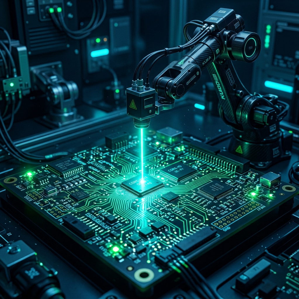
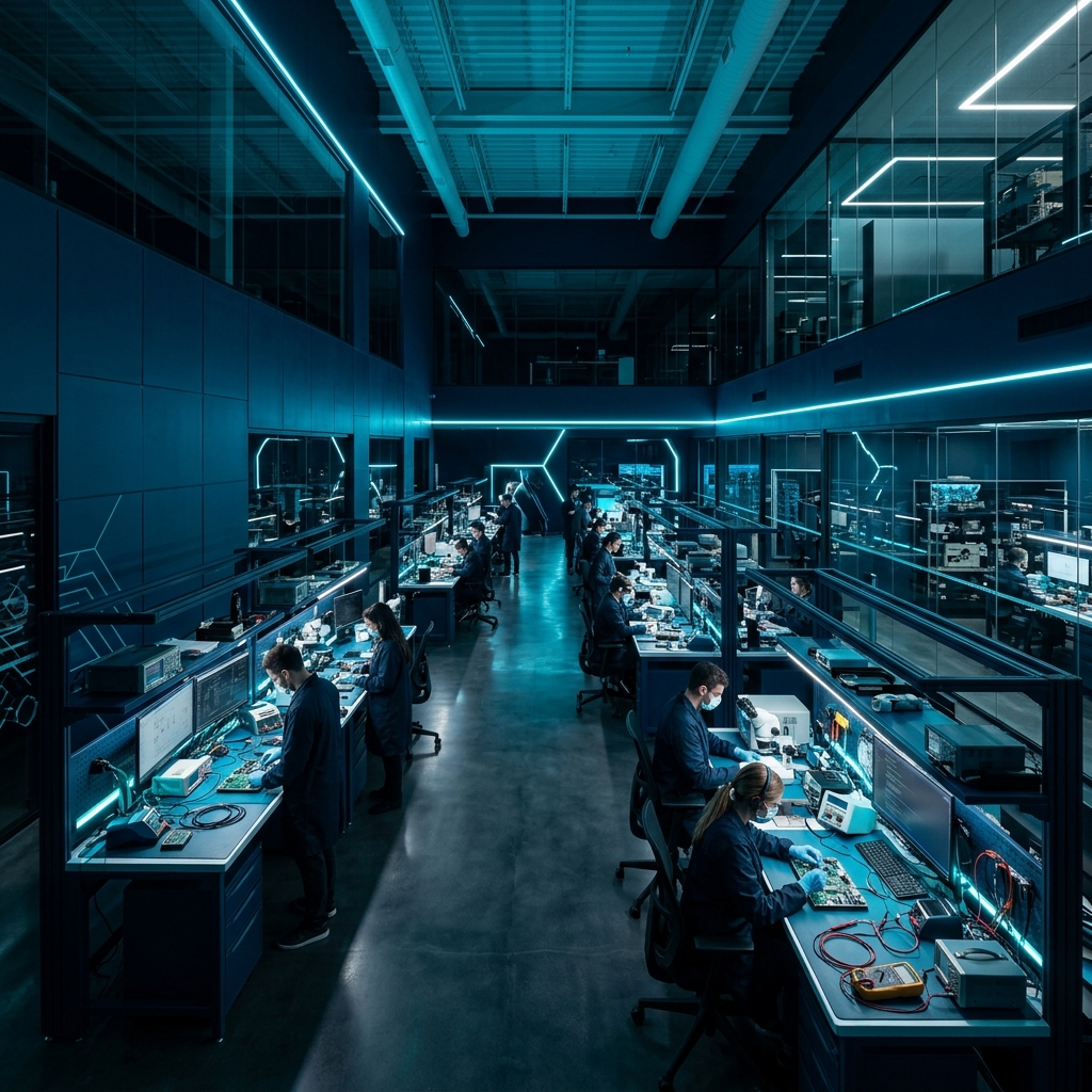
Advanced Manufacturing & Labs.
Take a look inside our high-tech assembly and engineering environments.
What the line is actually capable of.
Real figures we design against, not marketing rounding.
"We handed over a schematic and a deadline. I Assist (Pvt) Ltd came back with a routed, DFM-checked board and a working prototype nine days later — no back-and-forth on part substitutions or stackup guesses."
Send us the project, we'll send back a plan.
Attach a schematic, a rough sketch, or just a description of what the board needs to do — we'll follow up with scope, timeline and cost.